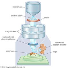
Scanning Electron Microscope (SEM):
Introduction:
Scanning Electron Microscope (SEM):
The scanning electron microscope (SEM) is a powerful scientific instrument that allows researchers to visualize and study the microscopic world with exceptional detail.
Unlike traditional optical microscopes, the SEM uses a beam of high-energy electrons to scan the surface of a sample, generating signals that form highly magnified images.
By harnessing the principles of electron-matter interactions, the SEM enables scientists to explore the topography, composition, and structure of various materials at the nanoscale.
This groundbreaking technology has revolutionized fields such as materials science, nanotechnology, life sciences, forensics, and art restoration, offering invaluable insights into the hidden realms of the microcosmos.
Principal:
The scanning electron microscope (SEM) operates on the principle of using a focused beam of high-energy electrons to examine the surface of a sample. Unlike traditional optical microscopes that use visible light, the SEM harnesses the unique properties of electrons to probe the microcosmos with exceptional resolution and depth.
The principle begins with an electron source, such as a tungsten filament or a field emission gun. When a voltage is applied, electrons are emitted from the source due to thermionic or field emission. These emitted electrons are then accelerated using electric fields toward the sample.
Electromagnetic lenses within the SEM play a vital role in focusing and directing the electron beam onto the sample's surface. By controlling the electromagnetic fields, the lenses ensure precise positioning and fine-tuning of the beam.
Before imaging, the sample needs careful preparation. It is typically cleaned, dehydrated, and coated with a thin layer of conducting material like gold or carbon. This coating helps reduce charging effects and enhances image quality.
Working:
The scanning electron microscope (SEM) works by using a beam of tiny particles called electrons to investigate the surface of a sample. This beam is created by an electron source and accelerated towards the sample using electric fields.
When the beam reaches the sample, it interacts with the surface, causing the emission of different signals. These signals, such as secondary electrons and backscattered electrons, are collected and converted into an image.
Secondary electrons provide information about the sample's surface features, while backscattered electrons reveal its composition. By analyzing these signals, scientists can obtain detailed images that show the texture, shape, and composition of the sample at a very high magnification.
The SEM allows researchers to explore the microscopic world and study a wide range of materials, from metals and ceramics to biological samples.
In simple terms, the SEM uses electrons to take close-up pictures of tiny things, showing us what they look like and what they're made of.
Application:
The scanning electron microscope has had a profound impact on numerous scientific disciplines, opening new frontiers of exploration and advancing our understanding of the microcosmos. Here are some notable applications:
SEM plays a crucial role in the characterization of materials, allowing scientists to examine their surface morphology, grain structure, and defects. It is instrumental in materials research and development, contributing to advancements in fields such as metallurgy, ceramics, and nanotechnology.
In biology and medicine, SEM aids in the study of cells, tissues, and organs. It provides detailed insights into cellular morphology, cellular interactions, and the structures of pathogens. SEM has also found applications in studying biomaterials and tissue engineering.
3) Nanotechnology:
SEM is an indispensable tool in the realm of nanotechnology, enabling scientists to visualize and manipulate nanostructures. It assists in the investigation of nanoparticles, nanowires, and nanotubes, paving the way for breakthroughs in electronics, photonics, and energy storage.
4) Forensics and Materials Analysis:
SEM is employed in forensic science to analyze trace evidence, such as fibers, particles, and tool marks. It helps identify and classify materials, aiding in criminal investigations. SEM is also valuable in failure analysis, allowing scientists to study fractured surfaces and determine the causes of material failures.
 |
| Tendons: Scanning Electron Microscope |
Advantages:
1) High Magnification and Resolution: The scanning electron microscope (SEM) provides extremely detailed images with high magnification, allowing scientists to see tiny structures and features that would be impossible to observe with other microscopes.
2) Versatility: SEM can analyze a wide range of materials, including metals, minerals, biological samples, and more. It offers valuable insights into the surface topography, composition, and elemental distribution of various substances.
3) 3D Imaging: SEM can generate three-dimensional images, providing a better understanding of the sample's shape, texture, and surface characteristics. This is particularly useful for studying complex structures and analyzing surface roughness.
4) Elemental Analysis: The SEM can identify the elements present in a sample by detecting characteristic X-rays emitted during electron-sample interactions. This enables researchers to determine the chemical composition and elemental distribution of the material being examined.
Disadvantages:
1) Sample Preparation: Samples for SEM analysis require careful preparation, including dehydration and coating with a conductive material. This process can be time-consuming and may introduce artifacts that affect the sample's natural state.
2) Vacuum Environment: SEM operates in a high vacuum environment, which limits the analysis of volatile or sensitive samples. Some samples may undergo changes or degradation under vacuum conditions, making it challenging to study certain materials.
3) Sample Size: The size of the sample that can be analyzed in an SEM is typically limited. Large or bulky samples may need to be sectioned or modified to fit within the microscope's chamber, potentially altering their original properties.
4) Cost and Accessibility: SEMs are complex and expensive instruments, requiring specialized facilities and trained personnel for operation and maintenance. This restricts their availability and accessibility to certain research institutions and organizations.
While the scanning electron microscope offers numerous advantages, it is essential to consider these limitations and ensure they are addressed appropriately to obtain accurate and reliable results.


0 Comments